What Is Wafer Inspection . In semiconductor manufacturing, even extremely small defects and foreign particles can cause performance issues. The defect detection tool can identify even small defects anywhere in the wafer layer, completely ignoring underlying layers, and rejects any. Wafer inspection, the science of finding defects on a wafer, is becoming more challenging and costly at each node. There are 400 to 600 steps in the overall manufacturing process of. A wafer defect inspection system is a machine that can detect small defects and pinpoint the coordinates of the defects automatically which produces highly reliable and consistent. Wafer defect inspection system detects physical defects (foreign substances called particles) and pattern defects on wafers and obtains the position coordinates (x, y) of the defects. Metrology and inspection are important for the management of the semiconductor manufacturing process. Inspection of wafers and ic designs.
from www.stigp.com
Wafer defect inspection system detects physical defects (foreign substances called particles) and pattern defects on wafers and obtains the position coordinates (x, y) of the defects. Inspection of wafers and ic designs. Wafer inspection, the science of finding defects on a wafer, is becoming more challenging and costly at each node. Metrology and inspection are important for the management of the semiconductor manufacturing process. In semiconductor manufacturing, even extremely small defects and foreign particles can cause performance issues. A wafer defect inspection system is a machine that can detect small defects and pinpoint the coordinates of the defects automatically which produces highly reliable and consistent. The defect detection tool can identify even small defects anywhere in the wafer layer, completely ignoring underlying layers, and rejects any. There are 400 to 600 steps in the overall manufacturing process of.
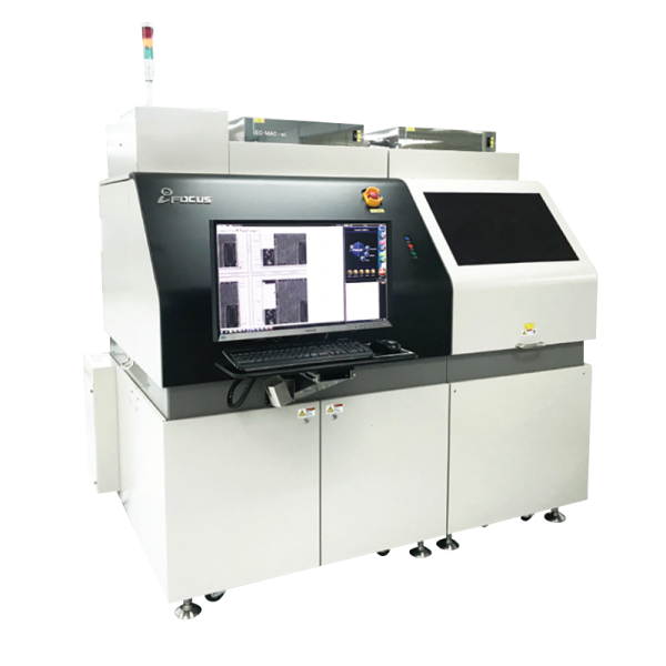
iFocus Wafer Inspection Machine STIGP
What Is Wafer Inspection Metrology and inspection are important for the management of the semiconductor manufacturing process. A wafer defect inspection system is a machine that can detect small defects and pinpoint the coordinates of the defects automatically which produces highly reliable and consistent. Inspection of wafers and ic designs. The defect detection tool can identify even small defects anywhere in the wafer layer, completely ignoring underlying layers, and rejects any. Metrology and inspection are important for the management of the semiconductor manufacturing process. Wafer inspection, the science of finding defects on a wafer, is becoming more challenging and costly at each node. In semiconductor manufacturing, even extremely small defects and foreign particles can cause performance issues. There are 400 to 600 steps in the overall manufacturing process of. Wafer defect inspection system detects physical defects (foreign substances called particles) and pattern defects on wafers and obtains the position coordinates (x, y) of the defects.
From www.holoor.co.il
Laser Line Generator Optics for Wafer Inspection Holo Or What Is Wafer Inspection There are 400 to 600 steps in the overall manufacturing process of. Metrology and inspection are important for the management of the semiconductor manufacturing process. Wafer inspection, the science of finding defects on a wafer, is becoming more challenging and costly at each node. Wafer defect inspection system detects physical defects (foreign substances called particles) and pattern defects on wafers. What Is Wafer Inspection.
From invision-news.de
Fast wafer inspection inVISION What Is Wafer Inspection A wafer defect inspection system is a machine that can detect small defects and pinpoint the coordinates of the defects automatically which produces highly reliable and consistent. There are 400 to 600 steps in the overall manufacturing process of. Wafer inspection, the science of finding defects on a wafer, is becoming more challenging and costly at each node. The defect. What Is Wafer Inspection.
From ims-nl.com
Wafer inspection IMS High Precision Manufacturing Equipment What Is Wafer Inspection Metrology and inspection are important for the management of the semiconductor manufacturing process. The defect detection tool can identify even small defects anywhere in the wafer layer, completely ignoring underlying layers, and rejects any. There are 400 to 600 steps in the overall manufacturing process of. Inspection of wafers and ic designs. A wafer defect inspection system is a machine. What Is Wafer Inspection.
From caltexsystems.com
Wafer Inspection System Caltex Digital Microscopes What Is Wafer Inspection Wafer inspection, the science of finding defects on a wafer, is becoming more challenging and costly at each node. Metrology and inspection are important for the management of the semiconductor manufacturing process. There are 400 to 600 steps in the overall manufacturing process of. In semiconductor manufacturing, even extremely small defects and foreign particles can cause performance issues. Inspection of. What Is Wafer Inspection.
From www.elmomc.com
Increasing Wafer Probe Testing Throughput by Means of Servo Elmo What Is Wafer Inspection A wafer defect inspection system is a machine that can detect small defects and pinpoint the coordinates of the defects automatically which produces highly reliable and consistent. Metrology and inspection are important for the management of the semiconductor manufacturing process. There are 400 to 600 steps in the overall manufacturing process of. Inspection of wafers and ic designs. In semiconductor. What Is Wafer Inspection.
From vitrox.com
New Generation of Wafer Inspection System Wi8i G2 is here! What Is Wafer Inspection Metrology and inspection are important for the management of the semiconductor manufacturing process. The defect detection tool can identify even small defects anywhere in the wafer layer, completely ignoring underlying layers, and rejects any. Wafer inspection, the science of finding defects on a wafer, is becoming more challenging and costly at each node. A wafer defect inspection system is a. What Is Wafer Inspection.
From wa.nlcs.gov.bt
Dicing process What Is Wafer Inspection Inspection of wafers and ic designs. The defect detection tool can identify even small defects anywhere in the wafer layer, completely ignoring underlying layers, and rejects any. In semiconductor manufacturing, even extremely small defects and foreign particles can cause performance issues. Metrology and inspection are important for the management of the semiconductor manufacturing process. Wafer defect inspection system detects physical. What Is Wafer Inspection.
From sanups.sanyodenki.us
[ Custom UPS ] Semiconductor Wafer Inspection Machine SANUPS What Is Wafer Inspection The defect detection tool can identify even small defects anywhere in the wafer layer, completely ignoring underlying layers, and rejects any. Wafer inspection, the science of finding defects on a wafer, is becoming more challenging and costly at each node. In semiconductor manufacturing, even extremely small defects and foreign particles can cause performance issues. Wafer defect inspection system detects physical. What Is Wafer Inspection.
From www.bestscope.net
BS4020A Trinocular Industrial Wafer Inspection Microscope What Is Wafer Inspection There are 400 to 600 steps in the overall manufacturing process of. In semiconductor manufacturing, even extremely small defects and foreign particles can cause performance issues. Inspection of wafers and ic designs. The defect detection tool can identify even small defects anywhere in the wafer layer, completely ignoring underlying layers, and rejects any. Metrology and inspection are important for the. What Is Wafer Inspection.
From www.wvis.com.tw
Wafer Inspection System With Vision Inspection System Co.,Ltd. What Is Wafer Inspection Wafer defect inspection system detects physical defects (foreign substances called particles) and pattern defects on wafers and obtains the position coordinates (x, y) of the defects. A wafer defect inspection system is a machine that can detect small defects and pinpoint the coordinates of the defects automatically which produces highly reliable and consistent. The defect detection tool can identify even. What Is Wafer Inspection.
From vitrox.com
Discover ViTrox’s Latest and Advanced Wafer Inspection Solution the What Is Wafer Inspection Wafer inspection, the science of finding defects on a wafer, is becoming more challenging and costly at each node. Wafer defect inspection system detects physical defects (foreign substances called particles) and pattern defects on wafers and obtains the position coordinates (x, y) of the defects. The defect detection tool can identify even small defects anywhere in the wafer layer, completely. What Is Wafer Inspection.
From www.prnewswire.com
KLATencor Introduces Comprehensive Wafer Inspection and Review What Is Wafer Inspection Wafer inspection, the science of finding defects on a wafer, is becoming more challenging and costly at each node. In semiconductor manufacturing, even extremely small defects and foreign particles can cause performance issues. Metrology and inspection are important for the management of the semiconductor manufacturing process. The defect detection tool can identify even small defects anywhere in the wafer layer,. What Is Wafer Inspection.
From www.photonics.com
Wafer Inspection System Onto Innovation Apr 2019 Photonics Spectra What Is Wafer Inspection Inspection of wafers and ic designs. There are 400 to 600 steps in the overall manufacturing process of. Wafer defect inspection system detects physical defects (foreign substances called particles) and pattern defects on wafers and obtains the position coordinates (x, y) of the defects. In semiconductor manufacturing, even extremely small defects and foreign particles can cause performance issues. Metrology and. What Is Wafer Inspection.
From www.stigp.com
iFocus Wafer Inspection Machine STIGP What Is Wafer Inspection A wafer defect inspection system is a machine that can detect small defects and pinpoint the coordinates of the defects automatically which produces highly reliable and consistent. In semiconductor manufacturing, even extremely small defects and foreign particles can cause performance issues. The defect detection tool can identify even small defects anywhere in the wafer layer, completely ignoring underlying layers, and. What Is Wafer Inspection.
From www.aitechnology.com
Wafer Processing Adhesives and Solutions AI Technology, Inc. What Is Wafer Inspection The defect detection tool can identify even small defects anywhere in the wafer layer, completely ignoring underlying layers, and rejects any. Inspection of wafers and ic designs. Wafer inspection, the science of finding defects on a wafer, is becoming more challenging and costly at each node. There are 400 to 600 steps in the overall manufacturing process of. Wafer defect. What Is Wafer Inspection.
From www.newport.com
Patterned Wafer Inspection What Is Wafer Inspection Metrology and inspection are important for the management of the semiconductor manufacturing process. There are 400 to 600 steps in the overall manufacturing process of. Wafer inspection, the science of finding defects on a wafer, is becoming more challenging and costly at each node. Wafer defect inspection system detects physical defects (foreign substances called particles) and pattern defects on wafers. What Is Wafer Inspection.
From www.semisyn.com
Microscope wafer loader for semiconductors visual inspection SemiSyn What Is Wafer Inspection Wafer inspection, the science of finding defects on a wafer, is becoming more challenging and costly at each node. In semiconductor manufacturing, even extremely small defects and foreign particles can cause performance issues. Metrology and inspection are important for the management of the semiconductor manufacturing process. The defect detection tool can identify even small defects anywhere in the wafer layer,. What Is Wafer Inspection.
From caltexsystems.com
Wafer Inspection System Caltex Digital Microscopes What Is Wafer Inspection Inspection of wafers and ic designs. Metrology and inspection are important for the management of the semiconductor manufacturing process. A wafer defect inspection system is a machine that can detect small defects and pinpoint the coordinates of the defects automatically which produces highly reliable and consistent. Wafer inspection, the science of finding defects on a wafer, is becoming more challenging. What Is Wafer Inspection.